
AI Vision for Electronics
High-precision inspection for PCB, soldering, and component assembly — sub-pixel accuracy at full line speed.
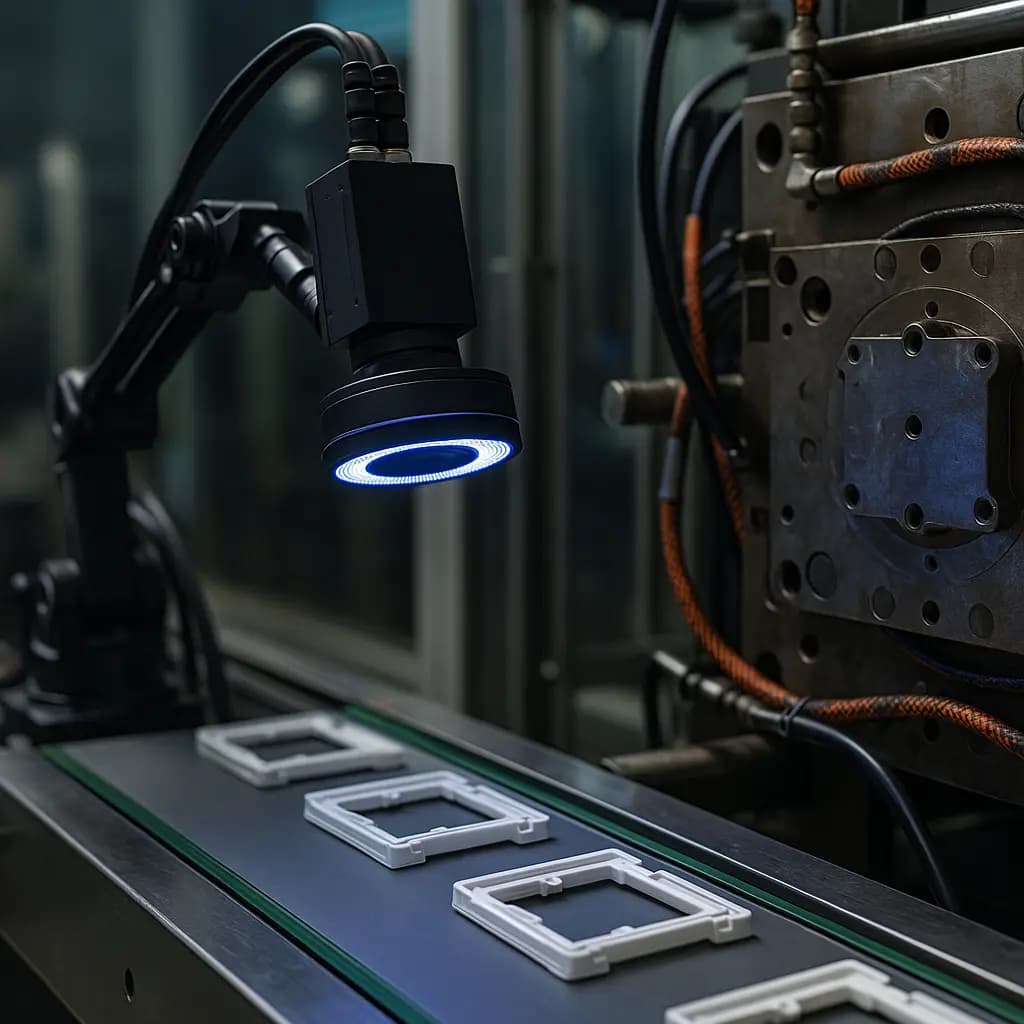
Engineered for every challenge in electronics inspection
If any of these sound like you — you're exactly who we help.
Sub-pixel solder joint inspection
Detect micro-cracks, cold joints, and misalignments across BGA, QFN, THT, and SMT — before they ship.
Real-time component verification
Live chip placement and orientation checks at full line speed — no blur, no compromise at 600+ ppm.
Adaptive multi-variant support
Handles new SKUs and board layouts instantly — no retraining, no reprogramming, no production delay.
What you're dealing with vs. what we deliver
See how OspreyX eliminates inspection pain points with smarter, production-ready AI vision.
"We miss tiny defects. Customers don't." — Legacy vision misses micro-cracks and misalignments.
We catch what others overlook — sub-pixel accuracy on micro-cracks, misalignments, and cold joints before they ship.
"Line speeds are too fast for inspection." — Traditional systems blur at 600+ ppm.
Our system sees every pad, pin, and trace clearly — at full line speed, no blur, no compromise.
"Every board variant breaks the model." — New SKUs crash fragile setups.
We adapt instantly to new SKUs and board variants — no retraining, no delay, no reprogramming.
"It flags everything — even good boards." — Too many false alarms stall production.
We detect true defects, not harmless variation — dramatically reducing false positives and line stops.
"We constantly tweak lighting and thresholds." — Manual tuning wastes hours every week.
Our system self-adjusts in real time — hands off. No manual lighting or threshold tuning required.
"Support takes too long. Lines go down." — Waiting days for help costs real money.
We respond within 24 hours — with real engineers, not ticket queues. Lines stay running.
Smarter vision systems for electronics manufacturing
Precision that never drifts
Sub-pixel AI inspection built for reflective coatings, transparent solder paste, and high-density boards — accurate under real factory conditions.
Deploy fast. Adapt instantly.
Pre-trained models handle multiple board layouts and component variants out of the box — no reprogramming when switching products.
Integrates with your line
Connects to SPI/AOI stations and MES systems with full traceability and defect classification — drop into existing workflows.
Frequently asked questions
Straight answers on platforms, integration, procurement, and support.
Speak with a vision engineer
Full-stack machine vision, engineered for real-world PCB and electronics production — not research labs.
High Accuracy from Day One
Solution Design
Transparent Pricing & Specs
Live Demo